Advanced Tutorial
Front and Back Layers
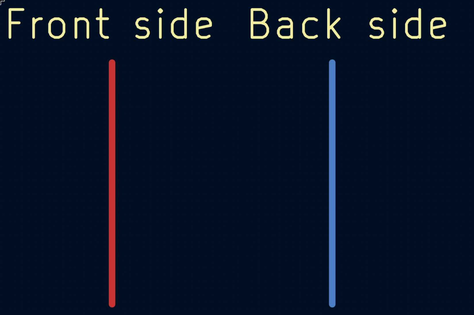
The PCBs we are making has 2 layers. You can tell if a pad or trace is on the front or back by it’s color: Red means front and blue means back.
You can also place components on both sides. To change the side which a component is on, click F. If you want to start drawing from the other side, click V and draw your traces normally. At last, traces can also switch sides in the middle of routing: press V to add a via, which will take your trace to the other side of the board.
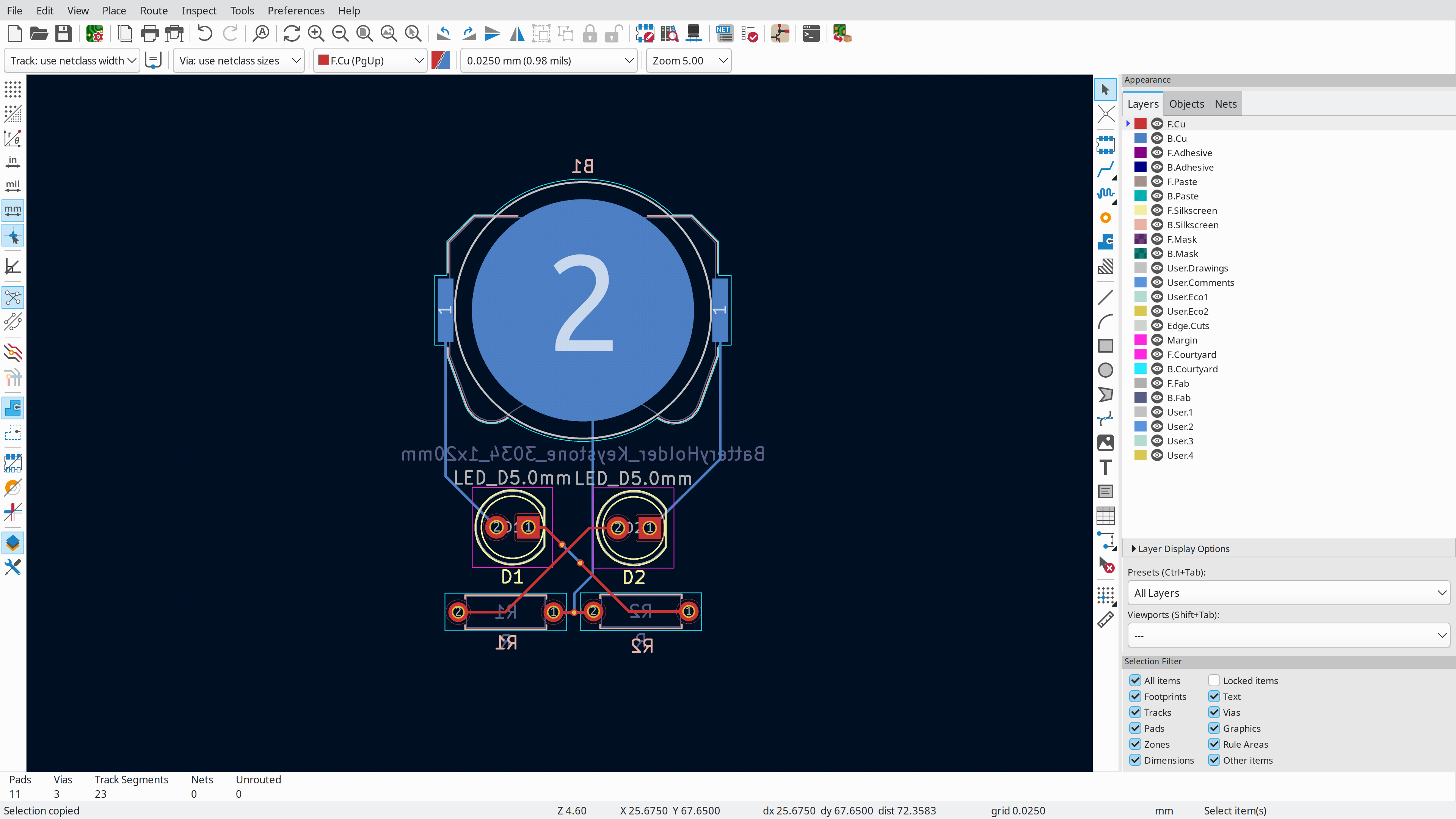
In the PCB above, we can see that the battery holder is blue, so it’s on the backside. The text of the resistors are of a darker yellow, so they are also on the back side.
Ground Pours
Routing all that GND traces is getting booring. How about we fill all the empty space with copper and get done with it?
Select Draw Filled Zones on the right, and press on one end of your board to start drawing. You will be prompted a menu, where you should check both “F.Cu” and “B.Cu”. On the Net menu, select GND and press ok. Now you can continue drawing a area around your PCB!
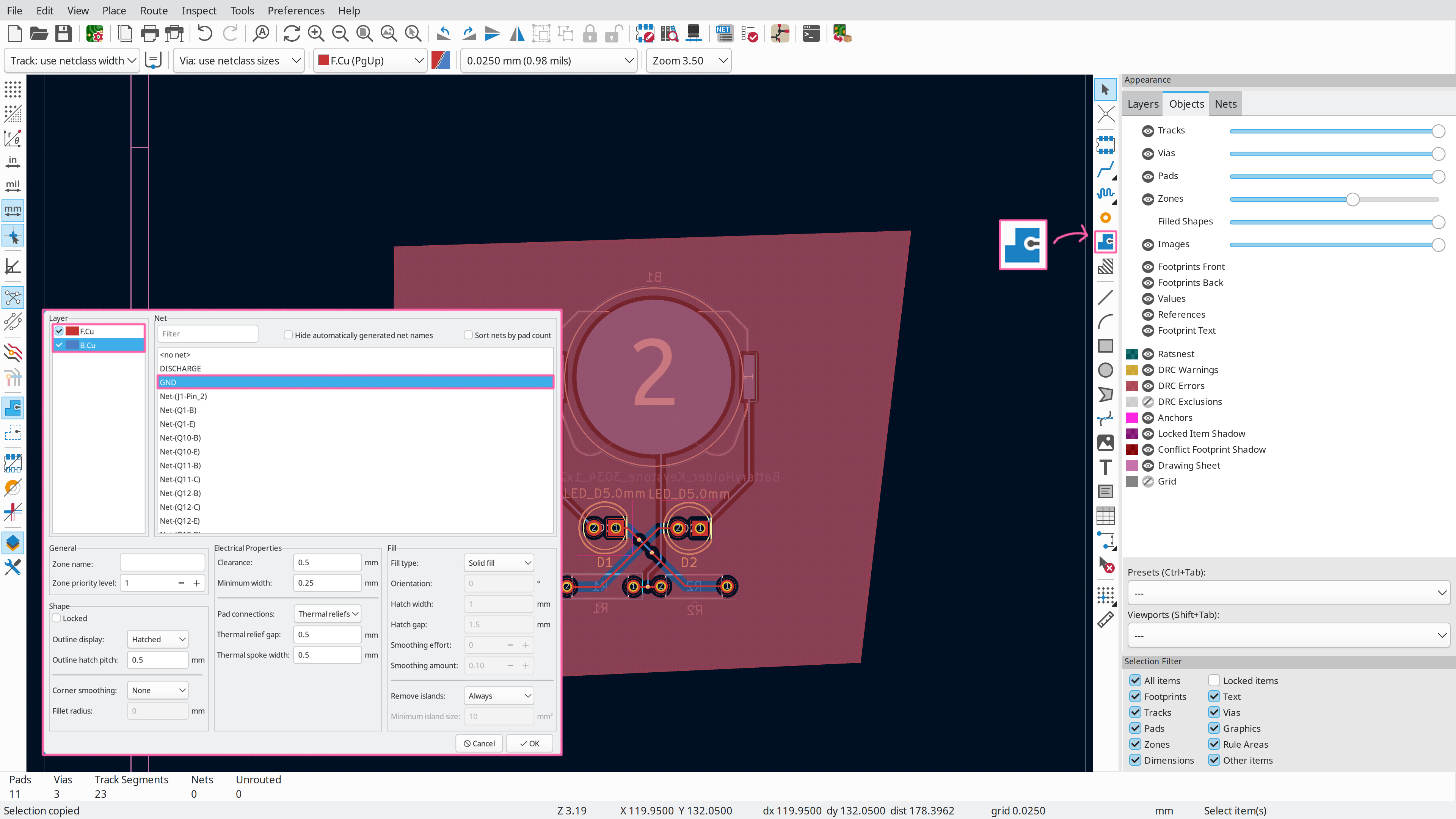
After that’s done, press B to fill your zone, and voila! Your ground pour is done, and you won’t need to route your ground.
Just one last thing: Press Control+Shift+X and place some vias all around your ground pour to conntect both sides of your board.
A Keychain Hole
If you want to add a keychain hole to the PCB, press control+shift+x to place a via, then press E and enter 5 for via hole, and 5.5 for via diameter! Now you have a plated hole :D